Other interfaces
Semiconductor electrodes
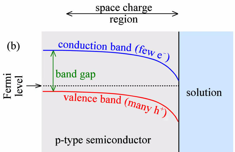
Semiconductor
- Lattice
- Valence band = HOMO (red on fig below)
- Conduction band = LUMO (blue on fig below)
- Band gap
- Fermio energy (chemical potential of electrons)
- Work function (to bring electrons to vacuum)
n-type semicond:
- Donor doped, n = [\(e^-\)] = [\(D^+\)]
- yields \(e^-\) in conduction band
- \(\mathrm{R}(a q) \rightleftarrows \mathrm{e}^{-}(s c)+\mathrm{O}(a q)\)
p-type semicond:
- Acceptor doped, p = [\(h^+] = [\)A^-$]
- yields holes in valence band
- \(\mathrm{R}(a q)+\mathrm{h}^{+}(s c) \rightleftarrows \mathrm{O}(a q)\)
Band bending can be because of 2 things:
- Adsorption of specific charged species on the surface of the electrode makes the fermi level change towards the surface.
- Alignment of Fermi levels
Electroosmotic drag
Charged walls of tube makes ions in fluid inside attracted to walls. When then put in an electric field, the areas of high density will be more affected by the field and move the fluid in the tube.
